As it would turn out, Amateur radio is a hobby pursued by many people who are interested in Electronics. I have always had a fascination for all things electrical in nature, and have spent my whole life making gadgets.
One of my many hobbies is music synthesis, and I derive great enjoyment in both purchasing and developing Eurorack modules for my home made synthesiser. I am so passionate about Eurorack, that I and working towards building a separate business that develops and manufactures interesting modules.
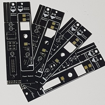
Genesis Modules has been active for a couple of years now, and I have completed a number of projects, but I thought that I would focus on a simple power control module, and the associated learning that I have been able to do in bringing that module to market. I will be open and honest, and say that I have made silly mistakes in the development of this board, but this article will help me clarify the checklist of things that I check before I ship a board to manufacture to ensure that there is a 100% likelihood it will work correctly.
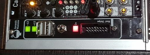
My first version of this board was developed in late 2018, driven from my need to have a simple switched power source from my eurorack chassis, so that I can power modules that are under test external to the rack, allowing me to probe points with oscilloscopes or signal generators. I made a simple board that provided a couple of voltage comparators to validate that +12 and -12V were correct (The associated LED would turn on when the voltage got to within 10%), as well as a switched output that provided a Eurorack standard 16 pin power connector, switching the +/- 12V supply. It also was polyfuse and polarity protected.
I was in the middle of my ‘Everybody Needs Orange Modules” phase at that stage, so it got a beautiful orange laser cut acrylic faceplate, and it lived in my rack for over a year, helping with the development of other modules.
Task accomplished! Or so I thought – it turned out that in the meantime, I bought a couple of interesting Roland devices that were powered by +5V USB power. So I had a couple of USB power adapters in a powerboard behind the rack, and all was good. This was ok – but something grated inside me and I felt that because I had perfectly good 5V in the rack, perhaps I should modify my power module to supply the much needed USB power.
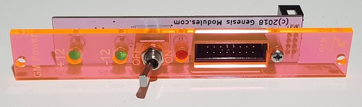
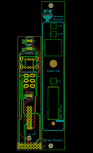
Easy. An evening with Kicad, and I had a neat board that even included a beautiful PCB based front panel. I had been wanting to replicate some of the beautiful PCB based panels that I had seen on other companies modules, so I carefully added a panel to the side of my finished PCB artwork. This would officially signal the start of my LEDs should glow softly behind a piece of PCB material that allows light through because it has an etched square shape phase. Beautiful!!! I even simplified the board, making the power LEDs simple indicators, stripping out the comparators, allowing space for the new USB socket.
The next day, I sent the board design out to a fabricator, a set of 5 double sided boards with black solder mask, and white silkscreen would not cost too much and should arrive within a week. Not too bad, even in the midst of Covid-19. A few days later the dual USB sockets that I needed arrived as well. I was looking forward to a weekend, making a couple of modules.
The weekend arrived, and disaster…. The USB sockets that arrived had a different layout to the pinout that I had designed for. I could flip them over, but I would need to swap 5v and ground on the back of the board. Frustrating, but doable. Assembly continued, and I went to mount the module into the rack, and it was too tall. Disaster – I had to shave a full 4mm off the top of the board and drill a new mounting hole.
5 boards, junk. Admittedly because they were prototypes it didn’t cost a heap, but it cost in pride. What happened???? I got cocky, and decided that the functionality of this board was simply too easy, and I didn’t follow my simple PCB checklist. I transposed some numbers incorrectly into KiCad and the panel size was wrong. I made a design for a component that I didn’t have a good datasheet for, assuming that USB connectors are pretty much the same, and that I could easily modify the KiCad library part. Silly, numpty mistakes. So – What does my checklist look like?
Checklists are fun!
For future reference, here is my checklist of common issues to check for on new PCBs. Doing everything here won’t guarantee success, but it will prevent embarrassment.
For the Schematic Capture:
- Make the project first of a piece of Veroboard – A working circuit is a great place to start from.
- Capture the Schematic using your layout package.
- Place circuit blocks logically.
- Liberally use text blocks to describe circuit blocks.
- Double check power connections are where they should be.
- When doing your PCB layout – label external switches and potentiometers with their function on the ‘Value” field – This field is displayed on the Front and Rear FAB layers, and ensures that you place external components where you expect them on the board- It makes it hard to confuse D2 and D3, when D2 is +12V LED and D3 is Power Enable LED.
- Capture component packages and supplier part numbers at the Schematic stage – that makes the board layout easier.
For the PCB layout:
- Obtain all of the components before you start doing the layout. Component footprint errors are easy to make, and the professionalism of tools like KiCad provides a false sense of security that its all ok.
- Identify the size of the board, and use the PCB edges layer to bound it. Double check it is correct.
- When placing components – start with the user interface parts – Potentiometers, Switches, LEDs, Sockets – Lay them out on a coarse, uniform grid. then lock them in place. There is nothing more frustrating than a row of sockets with one 0.5mm to the left of the others.
- Place the rest of the components in a neat, logical layout – focusing on proximity to their active controls. Bypass capacitors go beside the component they are bypassing.
- layout power connections – Big, fat traces are your friend here.
- layout signal lines.
- Clean up silkscreens to make them logical and neat – all component labels in the same direction etc.
- Do a final Design Rule Check to make sure you have not passed a track too close to a pad or something like that.
- Double check the board size.
The Front Panel:
- Identify the size of the panel, and use the PCB edges layer to bound it. Double check it is correct.
- When placing cutouts for switches, measure shafts with verniers as you go – Don’t assume that they are 6mm.
- Start at the lowest externally accessible component on your PCB and place that on your panel – Ensure you leave enough room below it for the internal PCB to clear any mounting hardware.
- Use that component as a dimensional anchor, and layout all other externally accessible components relative to that.
- Make sure that LED illumination cutouts are blocked out on the top solder paste, top copper, bottom copper and bottom solder paste layers. Otherwise LED light wont make it through the panel.
- Place external mounting holes on the panel.
- Place text and graphics on the panel – double checking component functions.
- Do a 1:1 check plot of the board and panel, and remove any cutouts with an exacto knife. Lay the cutout panel against the PCB and make sure that the components line up.
- Double check components will fit on the check plot without obstruction.
- Double check the final panel size.
If you are fabricating for a large production run, there are issues you need to consider, such as pannelising boards; ensuring you have enough breakaway material around the board to allow Pick and Place assembly; Adding Fiducials for alignment; making solder paste screen layouts, etc. We are not considering these here, so don’t worry.
Save your files and have a sleep or two.
Finally
Have a once over of the board and panel, double checking sizes, placement, etc. Only once you are happy, send the board to the Fab house. Then when the boards come back, assemble and mount the panel, happy in the knowledge that it’s going to be right.

