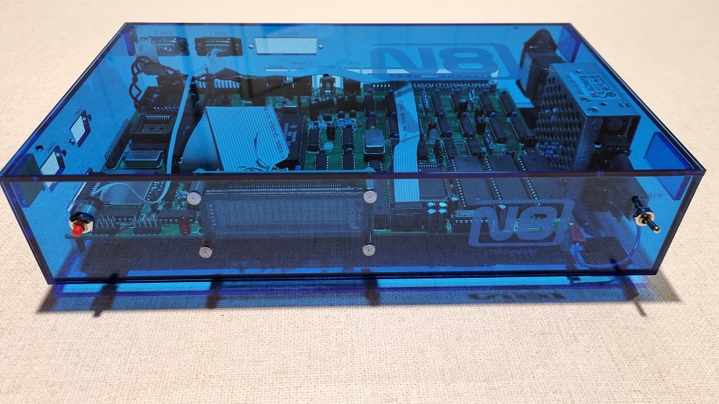
I recently decided to finish my Z180 based Single Board computer. It is a board named the “N8” designed in about 2012 as part of the then expanding N8VEM series of projects. It was neat because it promised to be able to run CP/M, have SD card support, 1Mb of actual RAM, 512K of Rom, and a couple of serial ports.
It also has MSX compatible TMS9918 Composite Color Video as well as an AY-3-8910 Sound Generator, and PS/2 Keyboard and Mouse if that floats your boat. My focus was on CP/M support, so I was not particularly concerned about the onboard NTSC video – It is a pain getting a composite CRT NTSC unit now days here in Australia.
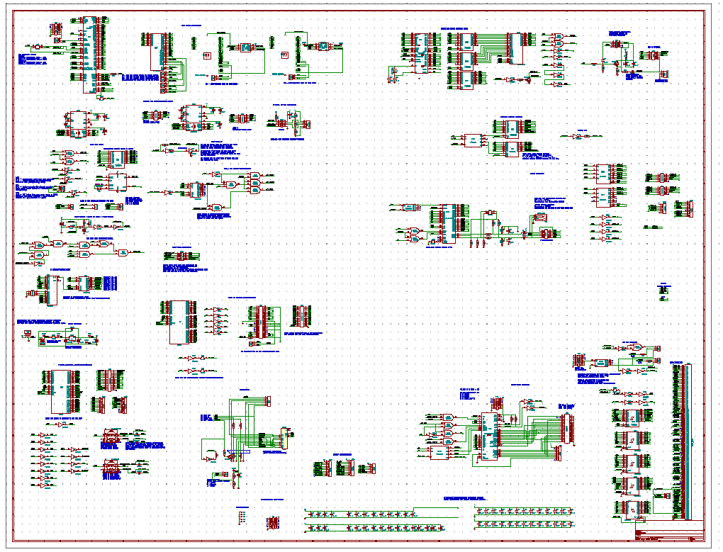
One of the things that I discovered was that these projects get orphaned fast, taking into consideration that it is basically 10 years since the project was developed – there is sparse doco on the web, and, at least for this version of the board, the schematics are a massive – single sheet with a really low resolution PDF file. At least some schematics are better than none.
One of the reality’s of the retro computers scene is that it moves fast – very bright individuals have an idea, they then spend the time to stand up the project up themselves doing the board design and layouts etc. A small community follows it for a while, the project goes through some iterations, getting better and better boards – Eventually, the next project is started and things slow down. This is not normally an issue, but in this case the person who spearheaded the N8 boards, as well as the Zeta board decided that he wanted to do something else (Which is awesome), and the projects – and associated mailing lists got moved into an archive.
There are a number of brilliant support groups, but you do have to focus a little to keep track of where they are – I was fortunate that I had a solid link into the S100 microcomputer scene, which is very similar, and there were people there who could support me, so I dropped a couple of messages there, and got some ideas for progressing.
Anyhow – I digress.
When I completed the board, I left out the Video and audio devices, as well as the video RAM, intending to load RomWBW into it for testing. The RomWBW image was built – a serial terminal was added and I hit the power… and Nada… Nothing… Zip…. Sigh…. Now I was in uncharted territory – I could not simply plug in my Z180 emulation pod to do some faultfinding – All fault finding would have to be done the hard way, by writing short programs and looking at what happened on the bus.
First thing – Write a program to Jump back to 0000 – “C3 00 00”. Loaded that into ROM and started it. A quick look with a logic analyser showed that it was indeed executing the program and jumping back to address zero. Wohoo.
Second thing – The RomWBW starts by copying itself into RAM to execute – The Z180 has the ability to map 1Mb of external address space into a 64k Z80 Range – watching the bus while it did that, there was certainly a period while it copied the software, a period where it only accessed RAM, and then it looked like it was starting all over again. Bummer. May be a memory decode style fault. I needed some sort of ability to output some diag data – anything.
Status LED
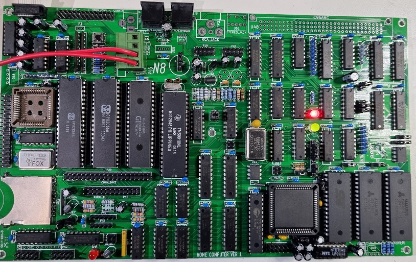
I need eyes – As I mentioned before I don’t have an emulation pod, so I would love to have a simple blinky LED. Hmmmm…. It turns out that onboard there is a STATUS LED I chose a big, shiny, classic RED LED for it when I populated the board – It is connected to the Auxiliary Control Register (*ACRCS) – Bit 3. So I write a quick test program to toggle that LED, with a delay – and was greeted with a slowly blinking Status LED –
DEPLOY THE SNOOPY DANCE!!!!
For completeness, here is a test program that I used for this. Yes – there is duplication with the delay routine, but I think linearly, and I can’t rely on RAM, therefore there is no stack, so I can’t call a subroutine.
ACRCS	.EQU $94	; Auxiliary Control register
STATUS_ON	.EQU	$1B	; 00011011   bit pattern to turn on STATUS LED
STATUS_OFF	.EQU	$13	; 00010011   bit pattern to turn off STATUS LED


	.ORG	0
	DI 			; disable interrupts

	LD BC, 0010h            ;Loads BC with hex 0010
Outer0:
	LD DE, 1000h            ;Loads DE with hex 1000
Inner0:
	DEC DE                  ;Decrements DE
	LD A, D                 ;Copies D into A
	OR E                    ;Bitwise OR of E with A (now, A = D | E)
	JP NZ, Inner0           ;Jumps back to Inner0 label if A is not zero
	DEC BC                  ;Decrements BC
	LD A, B                 ;Copies B into A
	OR C                    ;Bitwise OR of C with A (now, A = B | C)
	JP NZ, Outer0           ;Jumps back to Outer0 label if A is not zero

	LD  A, STATUS_ON        ; Turn on Status LED
	OUT0 (ACRCS),A


	LD BC, 0010h            ;Loads BC with hex 0010
Outer:
	LD DE, 1000h            ;Loads DE with hex 1000
Inner:
	DEC DE                  ;Decrements DE
	LD A, D                 ;Copies D into A
	OR E                    ;Bitwise OR of E with A (now, A = D | E)
	JP NZ, Inner            ;Jumps back to Inner label if A is not zero
	DEC BC                  ;Decrements BC
	LD A, B                 ;Copies B into A
	OR C                    ;Bitwise OR of C with A (now, A = B | C)
	JP NZ, Outer            ;Jumps back to Outer: label if A is not zero

	LD  A, STATUS_OFF
	OUT0 (ACRCS),A

	JP $0000

	.END
Wohoo – again – I have a simple diagnostic indicator – now can I write to memory?
Writing to RAM
Now – we have proven that ROM reads work (at least in the first 100 or so bytes of ROM), and that we can write to the Aux Control Register. Next is to test the RAM. I have to learn about how memory management works on the Z180.
It turns out that it is surprisingly simple. There are a couple of registers CBAR, BBR, and CBR that define where in physical memory various blocks sit, as well as the size of those blocks. Julian Skidmore has a brilliant blog entry that describes how it works (http://oneweekwonder.blogspot.com/2017/12/z180-mmu-tiny.html)
So – I defined a 32k split that started ram at 0x8000 and mapped it to 0x80000, utilising the second 512k RAm chip. Then I expanded the flashing program to write a byte to memory, and read it back – if it read back currently emit a flash – otherwise no flash. And It ran – and flashed. I also monitored the Chip Select pin on the RAM chip, and it pulsed in line with the writes and reads. Success. Memory works.
; test program to validate writing to RAM

Z180_BASE	.EQU	$40
Z180_ICR 	.EQU	$3f
Z180_RCR	.EQU	$76
Z180_TCR	.EQU	$50
Z180_ITC	.EQU	$74
Z180_CMR	.EQU	$5e
Z180_CCR	.EQU	$5f
Z180_DCNTL	.EQU	$72
Z180_CBAR	.EQU	$7a
Z180_BBR	.EQU	$79
Z180_CBR	.EQU	$78

ACRCS	.EQU $94	; Auxiliary Control register
STATUS_ON	.EQU	$1B	; 00011011   bit pattern to turn on STATUS LED
STATUS_OFF	.EQU	$13	; 00010011   bit pattern to turn off STATUS LED


	.ORG	0
	DI 			; disable interrupts


	LD	A,Z180_BASE
	OUT0	(Z180_ICR),A

		; DISABLE REFRESH
	XOR	A
	OUT0	(Z180_RCR),A

		; MASK OFF TIMER INTERRUPTS
	XOR	A
	OUT0	(Z180_TCR),A
	OUT0	(Z180_ITC),A

             	; SET DEFAULT CPU CLOCK MULTIPLIERS (XTAL / 2)

	XOR	A
	OUT0	(Z180_CMR),A
	OUT0	(Z180_CCR),A

            	; SET DEFAULT WAIT STATES
	LD	A,$F0
	OUT0	(Z180_DCNTL),A

	; Z180 MMU SETUP
	LD	A,$80
	OUT0	(Z180_CBAR),A		; SETUP FOR 32K/32K BANK CONFIG
	XOR	A
	OUT0	(Z180_BBR),A		; BANK BASE = 0
	LD	A, $F0
	OUT0	(Z180_CBR),A
	; end Z180 MMU SETUP


;!!!!!!!!!!!!!!!!!!!!!!!!!!!
;  Theoretically at this point, we have 32k of ram and 32k of rom!
;
; lets see.....  Can we still flash?  Yep
;
; Now - Lets see if we can write to $8000 - If that is RAM? Yep - we are triggering *CS on the sedond RAm chip
;  Now lets read back what we write and stop if we fail


aaaa:

	; write F0 to ram
	LD 	HL, $8000
	LD	A, $F0
	LD (HL),A

	;Read it back
	LD A, (HL)
	CP $F0
	JP NZ, BORKED	; skip turning on the LED

	LD	A, STATUS_ON		; Turn on the Status LED
	OUT0 (ACRCS),A

BORKED:

; Delay for a bit
	LD BC, 0010h            ;Loads BC with hex 0010
Outer0:
	LD DE, 1000h            ;Loads DE with hex 1000
Inner0:
	DEC DE                  ;Decrements DE
	LD A, D                 ;Copies D into A
	OR E                    ;Bitwise OR of E with A (now, A = D | E)
	JP NZ, Inner0           ;Jumps back to Inner: label if A is not zero
	DEC BC                  ;Decrements BC
	LD A, B                 ;Copies B into A
	OR C                    ;Bitwise OR of C with A (now, A = B | C)
	JP NZ, Outer0            ;Jumps back to Outer: label if A is not zero


	; write 0fh to ram
	LD 	HL, $8000
	LD	A, $0F
	LD (HL),A

	;Read it back
	LD A, (HL)
	CP $0F
	JP NZ, BORKED1	; skip turning on the LED

	LD	A, STATUS_OFF
	OUT0 (ACRCS),A

BORKED1:

; Delay for a bit
	LD BC, 0010h            ;Loads BC with hex 0010
Outer1:
	LD DE, 1000h            ;Loads DE with hex 1000
Inner1:
	DEC DE                  ;Decrements DE
	LD A, D                 ;Copies D into A
	OR E                    ;Bitwise OR of E with A (now, A = D | E)
	JP NZ, Inner1           ;Jumps back to Inner: label if A is not zero
	DEC BC                  ;Decrements BC
	LD A, B                 ;Copies B into A
	OR C                    ;Bitwise OR of C with A (now, A = B | C)
	JP NZ, Outer1           ;Jumps back to Outer: label if A is not zero

	JP aaaa

	.END
WOHOO!!!! I ran the test program and there was flashing. I changed the program to write to 0x7FFF and there was no flashing, proving that it couldn’t write to ROM, and verifying that my test program worked. I have now proven that the Z180 can read ROM, and can write (at least) to one byte of RAM.
Now – I have to prove I can write a serial character…..
This is just like testing an engine – Does it have air/fuel, does it have compression, does it have spark and finally is the spark at the correct time in the cycle. Yep to all, and VROOM!!!!!!!
Serial Ports
The Z180 has a couple of very capable ACSI ports (ACSI0, and ACSI1) – these are infinitely configurable, and the N8 board has onboard MAX232 drivers that do the level conversion to RS232 for me.
One thing that worried me was that when I was testing RomWBW, there was never any serial output – There was a bucket load of processing, but not a byte of output. Lets do some output with a short test program that I wrote:
Setting up the port is simple – there are a few registers that have to be loaded (CNTLA0, CNTLB0, ASEXT0 and CNTR)
CNTLA0 – turns on the transmitter and receiver, sets bits per character and parity configuration
CNTLB0 and CNTR – Sets the clock dividers for the Baud Rate Generator
ASEXT0 – Turn off CTS testing – This is important, Clear To Send isn’t always going to be connected, so we need the transmitter to simply transmit.
Then a quick program to send the letter ‘A’ to the serial port forever – and blink the status LED between each character.
	ld	a,$7C			; rcrv & xmtr on, clear errors, 8N1, RTS high
	out0	(CNTLA0),a		; do it
	ld	a,$21			; set dividers for 9600 baud (phi = 9.216 MHz)
	out0	(CNTLB0),a		; do it
	ld 	a,$20			; ignore CTS
	out0	(ASEXT0),a

	ld	a,$03			; set CSIO baud rate to /160
	out0	(CNTR),a		; do it

;
;  The following code sends an endless stream of 'A's to the terminal.
;  If you need a quick test to verify that you got through the reset
;  and initial configuration, uncomment this code, burn a ROM, and
;  try it.
;
loop:
	LD	A, STATUS_ON		; Turn on the Status LED
	OUT0	(ACRCS),A


; Delay for a bit
	LD BC, 0010h            ;Loads BC with hex 0010
Outer0:
	LD DE, 1000h            ;Loads DE with hex 1000
Inner0:
	DEC DE                  ;Decrements DE
	LD A, D                 ;Copies D into A
	OR E                    ;Bitwise OR of E with A (now, A = D | E)
	JP NZ, Inner0           ;Jumps back to Inner0: label if A is not zero
	DEC BC                  ;Decrements BC
	LD A, B                 ;Copies B into A
	OR C                    ;Bitwise OR of C with A (now, A = B | C)
	JP NZ, Outer0           ;Jumps back to Outer0: label if A is not zero

reset1:
	in0	a,(STAT0)	; get status of ASCI0
	and	$02			; test TDRE
	jr	z,reset1	; loop until TDRE=1
	ld	a,'A'		; move byte into A
	out0	(TDR0),a	; send byte to ASCI0

	NOP
	LD	A, STATUS_OFF
	OUT0 	(ACRCS),A
	jp	loop		; do forever
Running this – No blinking – No serial output. Yep – there is a serial sending issue.
I commented out the test that checked TDRE and ran the program – Success – serial output being send everywhere – So, the TDRE bit was never being cleared – so the serial port was never being allowed to send by hardware…..
No – Could it simply be that CTS is not clear – a simple serial issue? I jumpered the TTL CTS output of the MAX232 to ground with a simple jumper wire. and re-ran the test, and was rewarded by not only blinking of the Status LED, but a steady stream of ‘A’ characters on the terminal.
I re-read the data sheet, and confirmed that setting the ASEXT0 register was supposed to allow CTS to be ignored. Maybe my Z180 doesn’t have that actual instruction (There are variants – lets look at that later)
I quickly burnt a fresh copy of RomWBW, and put it into the board and powered it up.
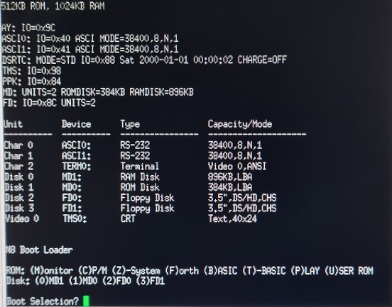
SUCCESS – What a journey. It simply turned out that my Z180 paid attention to the Serial CTS line, and wasn’t sending data.
Now – to understand the diferences between the N8-2511 and N8-2312 – Evidently the SD card interface was changed significantly. It should not be a complex set of mods, just cut a couple of traces, and jumper a couple of wires. I am not complaining, as the N8 project ran for a number of years, and I was an early adopter with the 2511 PCB, so of course there are changes.
In all a worthwhile block of time.


Did you know the N8VEM project just went under? Now how am I going to get support for my build? – I might need your help in the near future. I’m building this exact board.
The N8VEM projects were re-labeled, as Andrew didn’t want his callsign associated with the project anymore – he wanted some personal separation.
Thats totally up to him – I am happy to assign my name and callsign to projects forever, but some people decide that they want a break.
I wouold never say that the project ‘went under’ – instead, it is still fully comunity supported. It runs RomWBW – and that is under constant build and upgrade – with this board being one of the supported boards, so don’t despair.
If you need help from the comunity, just ask.